- Home
- Al Platforms
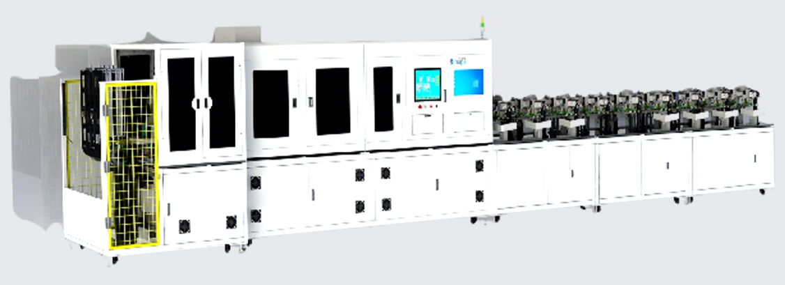
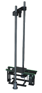
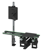
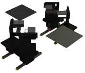
- AI Equipments
-
Solutions
- Machine Vision & Deep Learning
- 3D Vision & Smart Guidance
- Big Data & Machine Learning
- Partners
- News
- Career
- About Us